

Revenue, 2025
$ 40.5 Bn
Forecast, 2035
$73.9 Bn
CAGR, 2025-2035
6.2%
Report Coverage
Global
Market Size and Forecast
The Global Photoresist Chemicals Market was worth USD 40.5 billion in 2025 and is expected to reach USD 73.9 billion by 2035, growing at a CAGR of 6.2% from 2025 to 2035. Based on this growth rate, the market is estimated to reach around USD 43.8 billion in 2026. Asia Pacific held the largest regional share of 71.3% in 2025, valued at around USD 28.8 billion, supported by strong semiconductor fabrication, electronics manufacturing, display production, and advanced chipmaking investments.
The Photoresist Chemicals Market includes light-sensitive chemical materials used in photolithography to transfer circuit patterns onto semiconductor wafers and electronic substrates. These chemicals are widely used in integrated circuits, printed circuit boards, flat panel displays, MEMS devices, sensors, and advanced packaging. The market is closely linked with semiconductor production, miniaturization, cleanroom processing, and high-precision electronics manufacturing.
Key Parameter | Report Details |
|---|---|
Market Revenue, 2025 | USD 40.5 Billion |
Projected Revenue, 2035 | USD 73.9 Billion |
CAGR (2025-2035) | 6.2% |
Largest Region | Asia Pacific (71.3%, USD 28.8 Bn) |
Market Concentration | Medium |
Base Year | 2025 |
Forecast Period | 2025-2035 |
The market outlook remains steady as demand grows for smaller, faster, and more efficient electronic components. Growth can be attributed to rising semiconductor capacity, increasing use of advanced lithography materials, and strong demand from consumer electronics, automotive chips, and AI hardware. The expansion of Asia Pacific wafer fabs, specialty chemical supply chains, and next-generation chip technologies is expected to support long-term market demand.
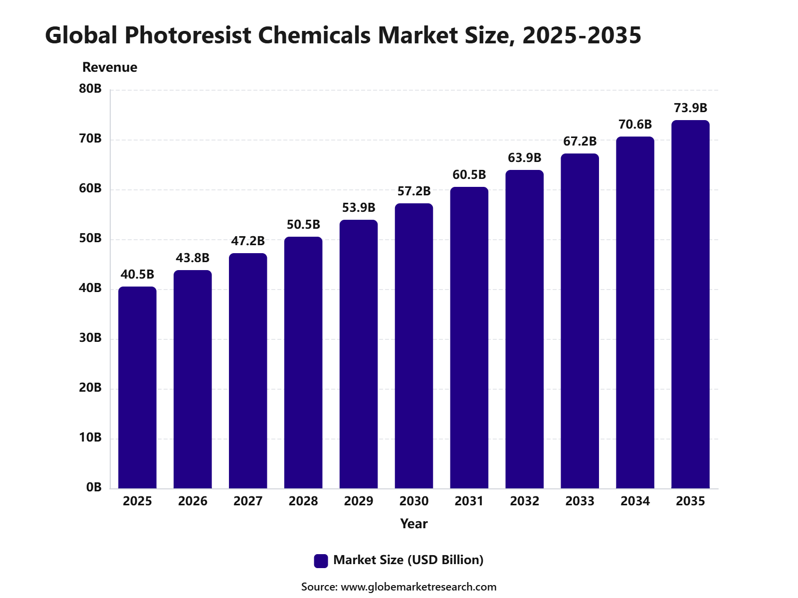 iThe graph shows projected market growth until 2035 based on CAGR analysis. Actual outcomes may vary depending on changing demand, competition, and economic factors.To gain greater insights - request a sample report PDF
Key Market Insights
DUV photoresists led the type segment with 44.1% share, supported by their strong use in advanced lithography, wafer patterning, and high-volume semiconductor manufacturing.
Semiconductors accounted for 65.3% share by application, driven by rising chip production, growing demand for microelectronics, and wider use of photoresist chemicals in integrated circuit fabrication.
Asia Pacific led the photoresist chemicals market with 71.3% share, valued at USD 28.8 billion, supported by large semiconductor fabrication capacity, strong electronics manufacturing, and expanding chip production across China, Taiwan, South Korea, Japan, and Southeast Asia.
Top Funding and Investment
Top Investment
In February 2026, Tokyo Ohka Kogyo reported construction of the world’s largest photoresist manufacturing building at its Koriyama Plant in Japan, with investment of over ¥20 billion.
In February 2026, Tokyo Ohka Kogyo reported construction of a high-purity chemical manufacturing building at TOKAM’s Pyeongtaek Plant in South Korea, with investment of about ¥12 billion.
In February 2026, Tokyo Ohka Kogyo reported a new inspection building at TOKAM’s Incheon Plant in South Korea, with investment of about ¥7 billion, supporting advanced semiconductor material quality control.
In early 2025, Fujifilm announced ¥4 billion investment at its Zwijndrecht site in Belgium to expand CMP slurries and photolithography developers, with operations planned from spring 2026.
In May 2026, JSR planned its first Taiwan photoresist production facility to supply and co-develop advanced photoresists with TSMC, with investment reported in the tens of millions of dollars.
Top Funding
In February 2025, Dongjin Semichem Texas received a $2.4 million Texas Semiconductor Innovation Fund grant for its Killeen specialty chemicals facility, supporting ultra-high-purity photoresist thinner production.
In February 2026, Irresistible Materials received a strategic financial investment from Tokyo Ohka Kogyo to advance its Multi-Trigger Resist EUV photoresist platform.
Top Acquisition
In February 2025, Tokyo Ohka Kogyo agreed to acquire all shares of Germany-based micro resist technology GmbH, adding a developer and producer of innovative photoresists, nanoimprint materials, and hybrid polymers.
By Type
DUV photoresists accounted for 44.1% share of the Photoresist Chemicals Market. This leading position is supported by their wide use in semiconductor manufacturing, especially in mature and advanced chip production processes where precise circuit patterning is required.
DUV photoresists are used in deep ultraviolet lithography to transfer fine patterns onto silicon wafers. These materials offer strong resolution, process stability, and compatibility with high-volume chip fabrication, making them important for logic chips, memory devices, sensors, and power electronics.
Demand for DUV photoresists is expected to remain strong as semiconductor production expands across consumer electronics, automotive electronics, data centers, artificial intelligence hardware, and industrial devices. Their established use in wafer processing supports continued adoption across major fabrication facilities.
By Application
Semiconductors accounted for 65.3% share of the Photoresist Chemicals Market. This dominance is driven by the critical role of photoresists in wafer patterning, circuit formation, etching control, and advanced lithography processes.
Photoresist chemicals are essential in manufacturing microchips, memory devices, processors, image sensors, power semiconductors, and display-related components. They help define extremely small circuit structures with high accuracy, which directly affects chip performance, yield, and reliability.
The segment is expected to remain the largest application area as demand rises for advanced computing, electric vehicles, 5G devices, smartphones, and connected industrial systems. Continued investment in semiconductor fabs will keep photoresist consumption strong across both advanced and mature process nodes.
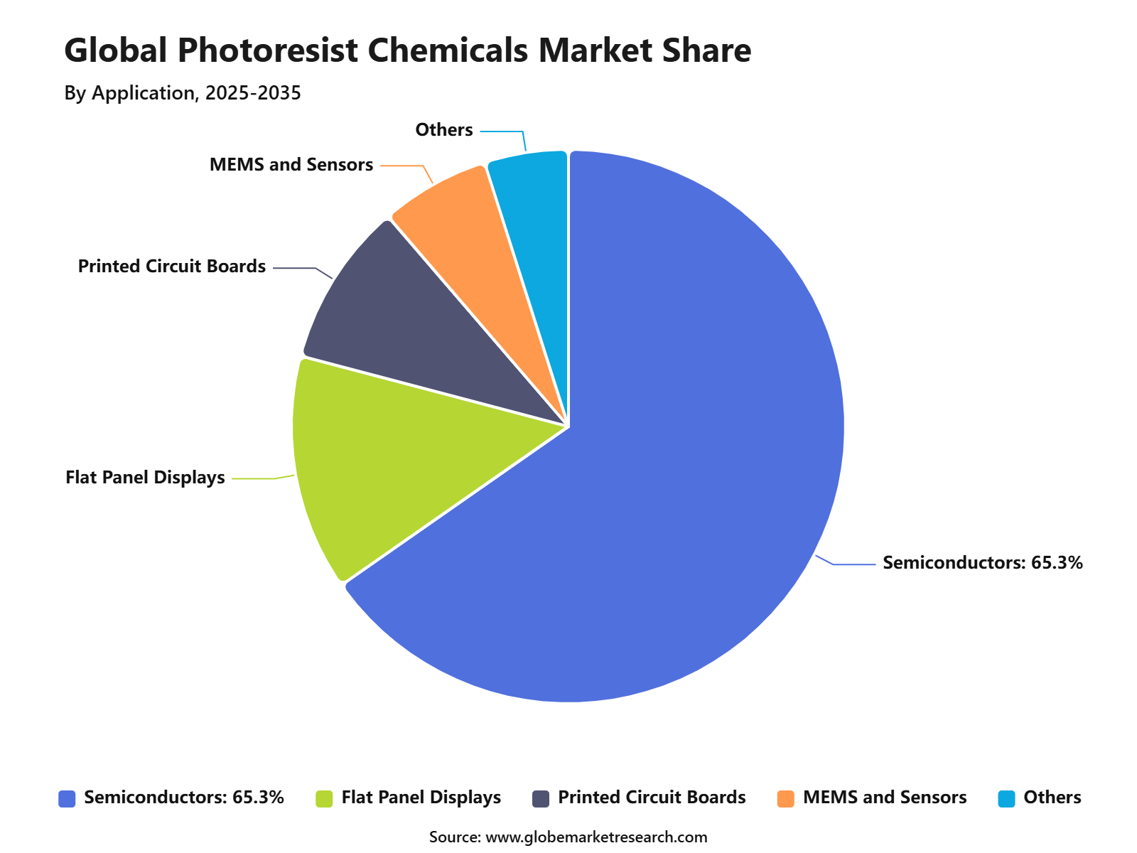 iThe graph shows projected market growth until 2035 based on CAGR analysis. Actual outcomes may vary depending on changing demand, competition, and economic factors.To gain greater insights - request a sample report PDF
By Region
Asia Pacific accounted for 71.3% share of the Photoresist Chemicals Market, reaching USD 28.8 billion. This leading position is supported by strong semiconductor fabrication, display panel production, electronics assembly, and advanced materials manufacturing across the region.
Taiwan, South Korea, China, Japan, and Southeast Asian countries are major contributors to regional demand. The region benefits from large chip manufacturing capacity, strong foundry operations, memory production, and high demand from consumer electronics and automotive electronics supply chains.
Asia Pacific is expected to maintain its leading position as semiconductor localization, AI chip demand, electric vehicle production, and electronics manufacturing continue to expand. Demand for DUV photoresists and other high-performance lithography chemicals will remain strong across regional fabrication hubs.
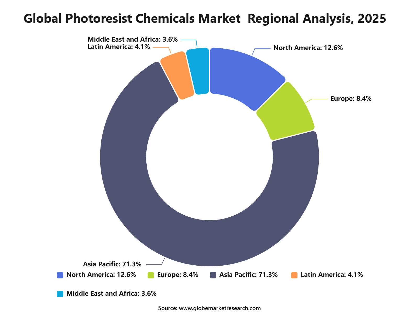 iThe graph shows projected market growth until 2035 based on CAGR analysis. Actual outcomes may vary depending on changing demand, competition, and economic factors.To gain greater insights - request a sample report PDF
Regional Impact Analysis
Asia Pacific leads the Photoresist Chemicals Market with 71.3% share in 2025, equal to about USD 28.9 billion, supported by semiconductor fabrication, display panel production, advanced electronics manufacturing, and strong supplier ecosystems. Taiwan, South Korea, Japan, China, and Southeast Asia remain major contributors.
North America remains important because of advanced chip design, semiconductor fabrication investment, and demand for secure domestic supply chains. Europe supports value growth through automotive semiconductors, specialty electronics, and advanced materials research.
Impact Factor | Estimated CAGR Impact | Regional Relevance | Market Impact |
|---|---|---|---|
Asia Pacific market leadership | +2.6% | Asia Pacific, 71.3% share in 2025 | Leads global demand. |
Taiwan and South Korea advanced fabs | +1.6% | Taiwan, South Korea | Drives premium consumption. |
Japan specialty chemical strength | +1.2% | Japan | Supports high-quality supply. |
China semiconductor and display expansion | +1.0% | China | Adds volume demand. |
North America and Europe fab investment | +0.8% | U.S., Germany, France | Supports supply |
Go-To-Market and Sales Economics
Photoresist chemicals are sold through direct fab qualification, long-term supply contracts, local technical centers, and electronics-material distributors. Demand is linked to advanced-node lithography, memory, high-performance computing, and AI chip production. SEMI reported that semiconductor materials revenue reached USD 73.2 billion in 2025, with wafer-fab materials at USD 45.8 billion.
Sales economics are supported by rising lithography intensity, tighter patterning requirements, and higher material consumption per wafer. SEMI expects worldwide 300mm fab equipment spending to rise 18% to USD 133 billion in 2026 and another 14% to USD 151 billion in 2027, supporting demand for EUV, ArF, KrF, and related ancillaries.
The go-to-market model must be close to fabs because customers need rapid sampling, defect analysis, purity control, and process tuning. TOK forecast FY2026 net sales of JPY 261.0 billion, up 10.1%, with electronic functional materials rising 12.3%. Front-end semiconductor photoresist sales are forecast to grow 10% year over year.
Risk Factors & Market Barriers
The largest barrier is qualification risk because photoresists must meet strict limits for particles, metals, line-width roughness, dose sensitivity, pattern collapse, and critical-dimension uniformity. JSR states that its ArF materials are designed for low defectivity, robust process latitude, low LWR, and excellent quality control, showing how technical performance controls supplier approval.
Export controls and equipment availability can affect demand timing. ASML reported Q1 2026 net sales of EUR 8.8 billion and expects 2026 sales of EUR 36 billion to EUR 40 billion, but stated that guidance includes possible outcomes from export-control discussions. This can influence lithography tool deployment and photoresist consumption by region.
Chemical regulation is another barrier because some semiconductor materials and process aids face environmental scrutiny, including PFAS-related substances in the wider electronics value chain. The semiconductor supply chain has warned that broad PFAS restrictions could affect materials used in consistent and safe chip manufacturing, making substitution, documentation, and waste handling important risks.
Revenue Potential Analysis
Revenue Landscape Across
Revenue is spread across EUV photoresists, ArF immersion resists, ArF dry resists, KrF resists, i-line resists, developers, anti-reflective coatings, hardmask materials, and packaging photoresists. JSR’s lithography portfolio covers i-line, KrF, DUV, and EUV photoresists, along with anti-reflective coatings, developers, multilayer hardmasks, and packaging materials.
Regional revenue is strongest in Asia because leading fabs and memory producers are concentrated there. SEMI reported Taiwan as the largest semiconductor-materials consumer for the 16th consecutive year in 2025, with USD 21.7 billion in revenue, followed by China at USD 15.6 billion and South Korea at USD 11.2 billion.
Customer revenue is also supported by strong foundry output. TSMC reported Q1 2026 net revenue of USD 35.90 billion, gross margin of 66.2%, and Q2 2026 revenue guidance of USD 39.0 billion to USD 40.2 billion. Strong advanced-node production supports steady demand for qualified photoresist and patterning chemicals.
Financial Impact
Photoresist chemicals create financial impact by improving yield, reducing rework, supporting smaller geometries, and enabling high-value chips. SEMI stated that lithography-related materials, including photomasks, photoresists, ancillaries, and wet chemicals, posted strong double-digit growth in 2025 due to higher process intensity and tighter lithography requirements.
Margins are protected when suppliers are qualified for advanced nodes because switching risk is high for fabs. Merck’s Semiconductor Solutions achieved 7.5% organic growth in Q1 2026, while Semiconductor Materials grew in the low-teens percentage range, supported by AI chip systems and advanced-node demand. This confirms stronger value in high-performance materials.
The strongest financial impact is expected from EUV and advanced ArF resists used in logic, DRAM, HBM, and advanced packaging flows. SIA stated that global chip sales remained on track to reach USD 1 trillion in 2026, which supports long-term demand for process-critical lithography chemicals across high-value semiconductor manufacturing.
Drivers Impact Analysis
The Photoresist Chemicals Market is driven by rising semiconductor production, advanced chip manufacturing, memory devices, logic chips, display panels, and printed circuit board applications. Photoresists are critical in photolithography, where they help transfer fine circuit patterns onto wafers and substrates.
Asia Pacific leads the market due to strong semiconductor fabrication capacity, advanced electronics manufacturing, and large chip supply chains. Taiwan, South Korea, Japan, China, and Southeast Asia remain key demand centers because of their strong wafer fabrication, foundry, display, and packaging ecosystems.
Impact Factor | Estimated CAGR Impact | Regional Relevance | Market Impact |
|---|---|---|---|
Rising semiconductor wafer fabrication | +1.7% | Asia Pacific, North America, Europe | Drives core photoresist demand. |
Growth in advanced logic and memory chips | +1.4% | Taiwan, South Korea, Japan, China | Supports high-performance chemicals. |
Expansion of consumer electronics production | +1.1% | Asia Pacific manufacturing hubs | Builds recurring demand. |
Growth in display panel manufacturing | +0.9% | China, South Korea, Japan | Adds specialty photoresist use. |
Demand for smaller semiconductor nodes | +0.8% | Advanced fabs globally | Supports premium formulations. |
Restraints Impact Analysis
The market faces restraints from high production complexity, strict purity requirements, and dependence on advanced semiconductor cycles. Photoresist chemicals must meet very tight quality, sensitivity, and contamination-control standards.
Another restraint is supply chain concentration. Since high-end photoresist production needs specialized raw materials, quality systems, and customer qualification, disruptions in materials or logistics can affect semiconductor manufacturing schedules.
Impact Factor | Estimated CAGR Impact | Regional Relevance | Market Impact |
|---|---|---|---|
High manufacturing and purification cost | -0.8% | Global producers | Pressures margins. |
Strict quality and contamination standards | -0.7% | Semiconductor fabs | Raises production complexity. |
Semiconductor demand cyclicality | -0.6% | Global chip markets | Affects order stability. |
Raw material supply concentration | -0.5% | Asia Pacific and Japan-linked supply chains | Creates supply risk. |
Long customer qualification timelines | -0.4% | Advanced chip manufacturers | Slows supplier switching. |
Opportunities Impact Analysis
Opportunities are strong in EUV photoresists, ArF immersion photoresists, KrF photoresists, advanced packaging photoresists, display photoresists, and high-purity ancillary chemicals. These areas benefit from rising chip complexity and expanding electronics production.
Higher-value opportunities are also emerging in next-generation semiconductor nodes, high-bandwidth memory, AI chips, 3D NAND, micro-LED displays, and advanced packaging. Companies that provide reliable performance, low defectivity, and strong supply security can capture higher-value demand.
Impact Factor | Estimated CAGR Impact | Regional Relevance | Market Impact |
|---|---|---|---|
EUV photoresist development | +1.6% | Taiwan, South Korea, Japan, U.S. | Builds premium market value. |
ArF immersion photoresist demand | +1.3% | Advanced semiconductor fabs | Supports leading-node production. |
Advanced packaging applications | +1.1% | Asia Pacific and North America | Adds new growth area. |
Display photoresist expansion | +0.9% | China, South Korea, Japan | Supports panel manufacturing. |
High-purity ancillary chemicals | +0.7% | Semiconductor supply chains | Improves process reliability. |
Challenges Impact Analysis
The main challenge is achieving consistent performance at smaller process nodes. Advanced semiconductor manufacturing requires photoresists with precise resolution, sensitivity, adhesion, etch resistance, and low line-edge roughness.
Another challenge is reducing defect rates while maintaining production scalability. Even small impurity levels or performance variations can affect wafer yield, making quality control and process repeatability essential.
Impact Factor | Estimated CAGR Impact | Regional Relevance | Market Impact |
|---|---|---|---|
Meeting advanced node performance needs | -0.7% | Leading-edge fabs | Increases technical difficulty. |
Reducing defectivity in lithography | -0.6% | Semiconductor manufacturers | Protects wafer yield. |
Maintaining batch-to-batch consistency | -0.5% | Global photoresist suppliers | Affects customer qualification. |
Managing complex formulation chemistry | -0.5% | Specialty chemical producers | Raises development cost. |
Scaling next-generation materials | -0.4% | EUV and advanced packaging users | Slows commercialization. |
Segment Covered in the Report
By Type
DUV Photoresists
g-line / i-line Photoresists
EUV Photoresists
Others
By Application
Semiconductors
Flat Panel Displays
Printed Circuit Boards
MEMS and Sensors
Others
By Region
North America
Europe
Asia Pacific
Latin America
Middle East and Africa
Market Trend Analysis
The market trend is moving toward EUV photoresists, advanced ArF formulations, low-defect photoresists, high-purity developers, edge bead removers, and specialty lithography materials. Demand is increasing as chipmakers invest in smaller nodes and higher device density.
Asia Pacific remains the leading demand region because most global wafer fabrication and electronics manufacturing capacity is concentrated there. North America and Europe are also gaining importance through semiconductor reshoring, advanced fab investment, and supply chain security programs.
Impact Factor | Estimated CAGR Impact | Regional Relevance | Market Impact |
|---|---|---|---|
EUV photoresist adoption increases | +1.5% | Taiwan, South Korea, Japan, U.S. | Supports leading-edge chips. |
Low-defect formulations gain demand | +1.2% | Advanced fabs globally | Improves wafer yield. |
Advanced packaging photoresists rise | +1.0% | Asia Pacific and U.S. | Adds process demand. |
Display lithography chemicals expand | +0.8% | China, South Korea, Japan | Supports panel production. |
Semiconductor supply localization grows | +0.7% | U.S., Europe, Asia Pacific | Improves supply resilience. |
Investor Type Impact Matrix
Investors should focus on photoresist chemical companies with strong purity control, advanced formulation capability, customer qualification history, clean packaging systems, and exposure to semiconductor and display manufacturers. Quality consistency and supply reliability are key success factors.
Strategic investors can also target EUV photoresist developers, high-purity chemical suppliers, lithography material producers, display photoresist companies, and semiconductor chemical distributors. Companies that reduce defects and support advanced node manufacturing are better positioned for long-term growth.
Investor Type | Estimated CAGR Impact | Regional Relevance | Market Impact |
|---|---|---|---|
Photoresist Chemical Producers | +1.5% | Global semiconductor hubs | Expands lithography material supply. |
EUV Photoresist Developers | +1.2% | Asia Pacific, U.S., Europe | Supports leading-edge chip growth. |
High-Purity Raw Material Suppliers | +1.0% | Japan, Asia Pacific, U.S., Europe | Strengthens supply reliability. |
Display Photoresist Manufacturers | +0.8% | China, South Korea, Japan | Adds specialty demand. |
Strategic Semiconductor Material Investors | +0.7% | Global chip supply chains | Funds advanced material capacity. |
Recent Developments
In May 2026, Allresist presented a new choline-based developer at EIPBN, positioned as a safer and more biodegradable alternative to conventional TMAH developers for lithography applications
In December 2025, Merck inaugurated its €500 million Kaohsiung semiconductor materials megasite in Taiwan, focused on thin films, formulation materials and specialty gases for advanced chip production.
In July 2025, Shin-Etsu’s annual report confirmed continued work in photoresists, photomask blanks, semiconductor silicon and encapsulant materials, supporting its electronics materials business for semiconductor manufacturing.
Competitive Landscape
The market is characterized by intense competition among established players and emerging companies. Strategic partnerships, mergers and acquisitions, and product innovation are key strategies employed by market participants.
Key Market Players
Tokyo Ohka Kogyo Co., Ltd.
JSR Corporation
Shin-Etsu Chemical Co., Ltd.
FUJIFILM Holdings Corporation
DuPont
Sumitomo Chemical Co., Ltd.
Mitsui Chemicals, Inc.
Allresist GmbH
Merck KGaA
KemLab Inc.
MicroChemicals GmbH
DONGJIN SEMICHEM Co., Ltd.
Other Key Players
Research Methodology
This market study is prepared using a combination of primary and secondary research. Primary research includes discussions with manufacturers, suppliers, distributors, consultants, industry experts, and end users. Secondary research covers company reports, government databases, trade associations, technical publications, regulatory sources, and trusted industry documents. The collected information is used to assess market demand, pricing trends, technology adoption, competitive activity, and regional performance.
AI language models are not used as primary data sources, and publicly available AI-generated content is not treated as market evidence. Computational tools may be used to support data processing, translation, data classification, and pattern identification. However, every published assessment is supported by verified sources, human review, and primary market discussions.
Market estimates are developed through top-down and bottom-up approaches and validated using data triangulation. Revenue, production, shipment, pricing, and application-level data are compared across multiple sources. Forecasts consider economic conditions, regulatory changes, investment activity, innovation, supply chain developments, and industry risks. All findings are reviewed through source verification and internal quality checks before publication.
Part I
Source Management & Input Data Standards
Who provides data, how sources are qualified, and what types of evidence are admissible.
Part II
Research Scope & Market Coverage
How we define the markets we assess and the parameters that govern each product.
Part III
Data Collection, Verification & Submission
The mechanics of gathering, cross-checking, and hierarchically ranking evidence.
Part IV
Assessment Determination & Quality Controls
How raw data becomes a published assessment — normalisation, expert judgement, and outlier exclusion.
Part V
Publication, Corrections & Revision
Our publication schedule, corrections policy, and methodology review cycle.
Part VI
Independence, Ethics & Complaints
Conflict-of-interest policies, editorial independence, and how clients raise concerns.
Google · Preferred Sources
Don't miss the latest market research insights and industry updates on Google.
Add Globe Market Research as a preferred source in the Google app to see our reports, analysis, and market stories in your news suggestions.
Meet the Team
This report was prepared by our expert analysts with deep industry knowledge and research experience.
Pratiksha K. is a Senior Research Analyst with more than five years of experience in market research, industry analysis, competitive intelligence, and business strategy. She has contributed to detailed market reports, customized research studies, company profiling, market sizing, trend analysis, and strategic consulting projects for clients across different regions. Her industry expertise covers Chemical and Material, Consumer Goods, Food & Beverages and Energy & Power. She closely evaluates changing customer requirements, technology developments, regulatory conditions, supply chain structures, investment activity, and competitive strategies to provide clear and practical market insights.
Sayali brings more than 7 years of experience to Globe Market Research, supporting the accuracy, clarity, and relevance of research content across multiple industries. She reviews market data, segment analysis, competitive insights, and industry trends to ensure each report meets strong quality standards and provides practical value to business decision-makers. Her expertise spans healthcare, information technology, consumer goods, and diverse cross-industry domains. With a strong focus on data reliability, structured analysis, and clear presentation, Sayali helps ensure that each research output delivers well-reviewed insights for clients, investors, consultants, and industry stakeholders.
Frequently Asked Questions
Related Reports
More in Chemical and Material
Sulfuric Acid Market to Hit USD 61.5 Billion by 2035
Sulfuric Acid Market Size, Share, Analysis By Raw Material (Elemental Sulfur, Base Metal Smelters, Pyrite Ore, Others), By Application (Fertilizers, Chemical Manufacturing, Metal Processing, Petroleum Refining, Textile, Automotive, Pulp and Paper, Others), By Distribution Channel (Direct Sales, Distributors), By Regional Insights, Business plan and Project Report, Investment Opportunities, Profitability, Industry Trends, Leading Companies and Growth Forecasts by 2026-2035
Powder Metallurgy Market to Hit USD 17.0 Billion by 2035
Powder Metallurgy Market Size, Share, Analysis By Material (Ferrous Metals, Non-Ferrous Metals, Others), By Process (Additive Manufacturing, Powder Metal Hot Isostatic Pressing, Conventional Powder Metallurgy), By Application (Automotive, Aerospace and Defense, Healthcare, Electrical and Electronics, Industrial Machinery, Others) , By Regional Insights, Business plan and Project Report, Investment Opportunities, Profitability, Industry Trends, Leading Companies and Growth Forecasts by 2026-2035
Bromine Market to Hit USD 1.5 Billion by 2035
Bromine Market Size, Share, Analysis By Derivative (Organobromine, Clear Brine Fluids, Hydrogen Bromide, Others), By Application (Flame Retardants, Oil and Gas Drilling, Biocides, PTA Synthesis, Plasma Etching, Pharmaceuticals, Energy Storage, Others), By End-Use Industry (Chemicals, Oil and Gas, Pharmaceuticals, Electrical and Electronics, Automotive, Agriculture, Others), By Regional Insights, Business plan and Project Report, Investment Opportunities, Profitability, Industry Trends, Leading Companies and Growth Forecasts by 2026-2035
Hydrogen Cyanide Market to Hit USD 5.95 Billion by 2035
Hydrogen Cyanide Market Size, Share, Analysis By Product Form (Hydrogen Cyanide Liquid, Hydrogen Cyanide Gas), By Application (Adiponitrile, Acetone Cyanohydrin, Sodium Cyanide and Potassium Cyanide, Methionine, Cyanuric Chloride, Others), By End-Use Industry (Chemicals, Mining and Metallurgy, Pharmaceuticals, Agriculture, Textiles, Others), By Regional Insights, Business plan and Project Report, Investment Opportunities, Profitability, Industry Trends, Leading Companies and Growth Forecasts by 2026-2035